
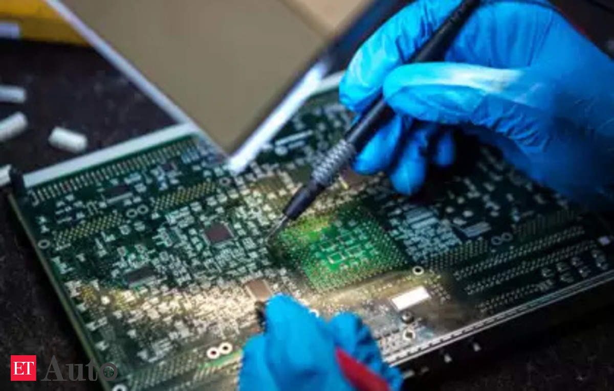
India will quickly begin making gear for semiconductor manufacturing, Union telecom and IT minister Ashwini Vaishnaw mentioned on Saturday.
“Your complete semiconductor ecosystem of fabs, ATMP models, chemical substances, gases, substrate, consumables and gear for semiconductor manufacturing will likely be made in India,” he mentioned.
He was talking on the inauguration of American chip gear provider Utilized Supplies’ India Validation Centre in Bengaluru which was arrange at a price of USD 20 million.
Such labs are current within the US, Singapore, China and Korea. The India Validation Centre may have a workforce of 500 folks.
The corporate final yr introduced that it’ll arrange an engineering centre in Bengaluru with a complete funding of USD 400 million over 4 years to develop and commercialise applied sciences for semiconductor manufacturing gear.
Vaishnaw mentioned that the elements that have been earlier imported from Japan, Korea and Taiwan are being made by the corporate right here now.
“At the moment, all of the 4 agreements made in the course of the Prime Minister’s state go to to the US have been materialised,” Vaishnaw mentioned.
The development of Micron’s ATMP has commenced. As well as, LAM Analysis’s proposal to ship a digital nano fabrication surroundings by means of its Semiverse Options to coach semiconductor engineers in India has additionally began.
“The primary coaching course within the Indian Institute of Science has began with 35 college students,” the minister mentioned. The third settlement was in relation to a centre of Utilized Supplies to be arrange in India, he mentioned. “This has additionally fructified with a centre of the corporate being arrange right here,” he mentioned.
A design centre of Superior Micro Gadgets (AMD) was additionally to be arrange in India. “A number of months again, I inaugurated the design centre of AMD in Bengaluru,” Vaishnaw mentioned.
A primary for 300 mm wafer processing
Sonny Kunnakkat, managing director, Superior Manufacturing Expertise, Worldwide Operations, Utilized Supplies, informed ET that that is the primary non-public facility in India that may course of 300 mm wafers.
Thus far, 200 mm wafers have been processed in India.
“We used to have a 300 mm processing facility within the Indian Institute of Expertise however that was educational. This can be a business one. We’ll do our personal improvement work. The wafers that we make will not be offered as we’re an gear firm and never a chip firm. Our gear right here will go to our prospects to make their chips,” Kunnakkat mentioned.
The change charge of the gear could be very quick, he mentioned. Gear and elements should be repeatedly developed with evolving buyer challenges. “That’s the type of improvement that will likely be accomplished right here,” he mentioned.


