

Renesas Electronics Company introduced that it’ll design 3-nanometer chips—an industry-first for the corporate—at its newly inaugurated Renesas Design Centre in Noida.
“We’re proud to announce that, for the primary time, 3-nanometer chips—an {industry} first—might be designed proper right here on the new Renesas Design Centre in Noida,” mentioned Malini Narayanamoorthi, India Nation Supervisor, Renesas Electronics Company. She added that the event marks a significant milestone in Renesas’ technique to construct for the world from India.
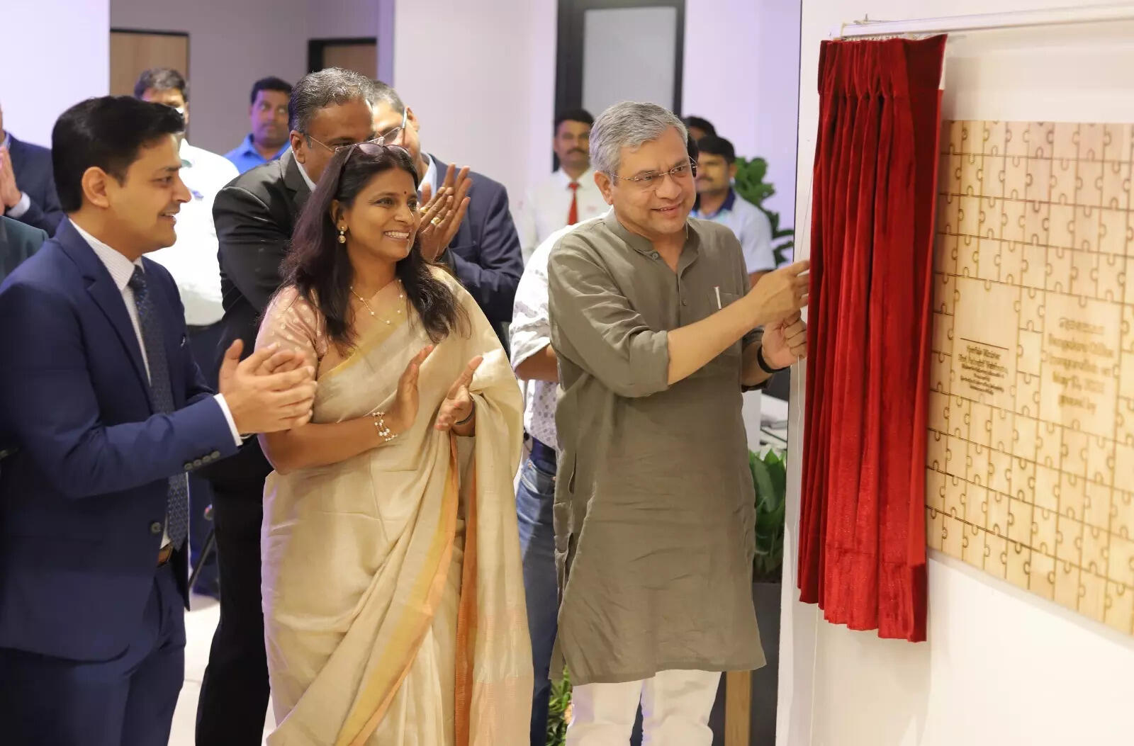
The announcement was made through the inauguration of Renesas’ new R&D services in Noida and Bengaluru, aimed toward strengthening its India operations and supporting the nation’s ambitions in semiconductor innovation. The Japan-based chipmaker additionally signed two MoUs with the Centre for Improvement of Superior Computing (C-DAC) underneath the Ministry of Electronics and Info Know-how’s Chips to Startup (C2S) programme to assist educational establishments and startups speed up chip design and embedded programs growth.
Talking on the Noida occasion, Ashwini Vaishnaw, Union Minister for Railways, I&B, and Electronics and IT, referred to as the collaboration “an important step” towards realising India’s purpose of changing into a semiconductor powerhouse.
Growth into superior design and expertise constructing
Renesas will present PCB design instruments and growth kits—together with entry to Altium Designer and the Altium 365 cloud platform—to over 250 educational establishments and 15 early-stage startups chosen underneath the C2S programme. This may facilitate experiential studying and fast-track product innovation amongst college students and entrepreneurs.
Malini highlighted that the corporate’s rising India presence isn’t just about capability, however functionality. “We’ve at all times been robust in system and product design. India affords a novel alternative to push the boundaries of innovation—from embedded software program to superior silicon design,” she informed ETAuto.
The newly opened Bengaluru facility has turn out to be Renesas’ largest web site in India with over 500 staff, together with R&D engineers, embedded software program groups, and professionals from its acquired companies Altium and Half Analytics. The centre might be pivotal in Renesas’ international product growth technique.
The Noida workplace, in the meantime, will function a design and buyer engagement hub, significantly centered on automotive, AI, and high-performance computing purposes. The centre will play a central function within the growth of Renesas’ flagship R-Automobile SoC platform for the automotive sector.
India-Japan Collaboration
Renesas CEO Hidetoshi Shibata, who joined the occasion nearly, described India as a “strategic cornerstone” within the firm’s roadmap. “From ideation to lifecycle administration, we purpose to construct a full-stack semiconductor ecosystem in India. This isn’t simply enlargement—it’s long-term collaboration,” he mentioned.
The corporate plans to scale its India workforce to 1,000 staff by the top of 2025, with operations throughout Noida, Bengaluru, Hyderabad, and Pune.
Along with the design centres, Renesas is engaged in an OSAT three way partnership with CG Energy and Stars Microelectronics in Gujarat and continues its educational partnerships, together with coursework packages at IIT Hyderabad.
Shibata emphasised the necessity to empower native innovation ecosystems, including, “By enabling startups and college students with the instruments they want, we’re serving to catalyze India’s subsequent era of semiconductor leaders.”


